Research
Research Focus
We develop advanced electron microscopy methods and apply them to understand materials from atomic structure and defects to functional properties and nanoscale electromagnetic states.
Ptychography & Quantitative Microscopy
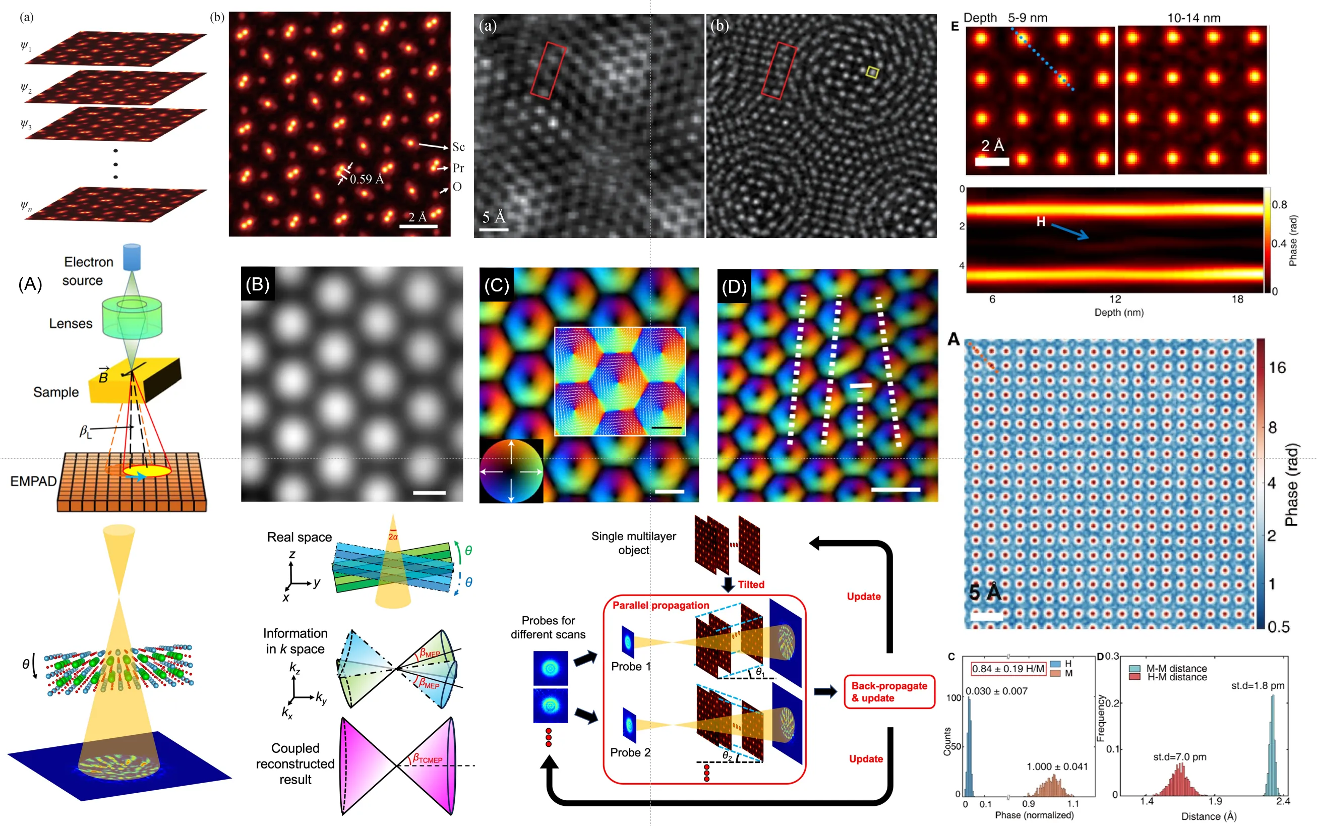
We develop electron ptychography and advanced 4D-STEM methods to push electron microscopy beyond conventional limits in spatial resolution, depth resolution, and quantitative accuracy. Our work has advanced multislice electron ptychography toward record-resolution and sub-picometer-scale structural measurement, three-dimensional atomic imaging, single-defect localization, and quantitative imaging of light elements, including oxygen and hydrogen in complex materials. By integrating high-speed detectors, energy filtering, cryogenic microscopy, computational imaging, and high-performance reconstruction algorithms, we aim to transform electron microscopy from primarily projection imaging into a quantitative, three-dimensional probe of atomic structure, composition, strain, polarization, and electromagnetic fields.
References
All publications →- Zhen Chen, Yi Jiang, Yu-Tsun Shao, et al. Science 372, 826 (2021).
- Zehao Dong, Yang Zhang, Chun-Chien Chiu, … Zhen Chen*, et al. Nature Communications 16, 1219 (2025).
- Huaicheng Yuan, Yu-Chen Liu, Li-Shu Wang, … Zehao Dong, Zhen Chen*, et al. arXiv (2025).
- Yi Jiang#, Zhen Chen#, Yimo Han, et al. Nature 559, 343 (2018).
- Zhen Chen*, Emrah Turgut, Yi Jiang, et al. Nature Nanotechnology 17, 1165 (2022).
- Zhen Chen, Matthew Weyland, Xiahan Sang, et al. Ultramicroscopy 168, 7 (2016).
Quantum & Functional Materials
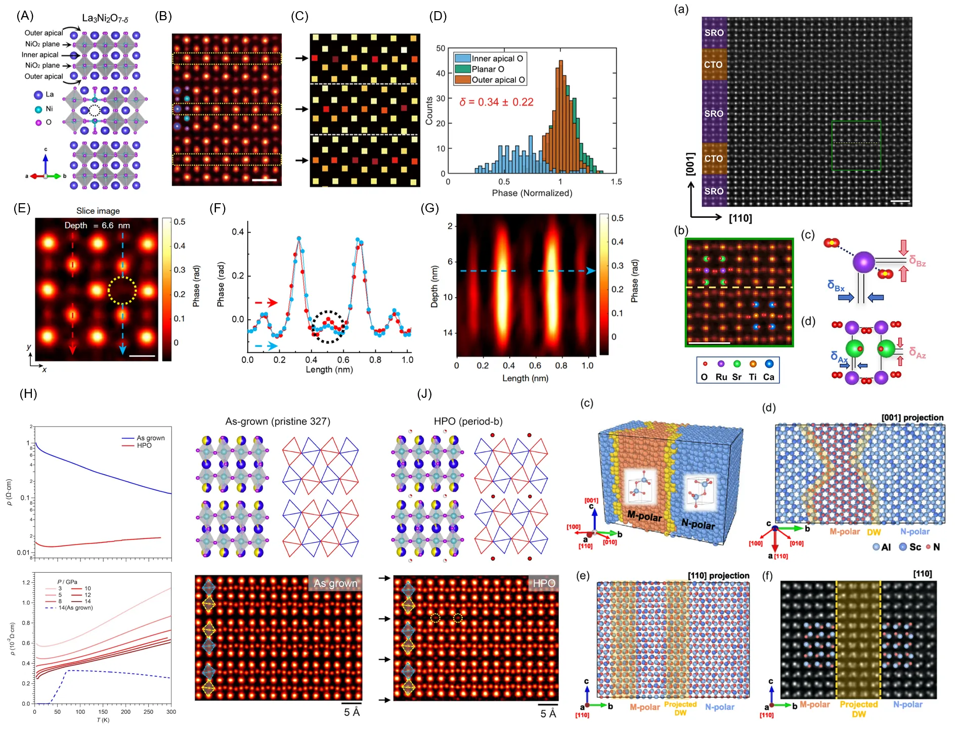
We use advanced electron microscopy to uncover the atomic-scale structural origins of emergent quantum phenomena. Our research spans correlated oxides, unconventional superconductors, charge-density-wave materials, low-dimensional systems, and other quantum materials in which subtle changes in atomic structure, defects, stoichiometry, and local symmetry can produce dramatic changes in electronic states. By directly mapping oxygen vacancies, lattice distortions, charge-order-related structural modulations, interfaces, and nanoscale heterogeneity, we seek to connect local atomic configurations with superconductivity, charge order, phase competition, and other collective phenomena, providing microscopic insight into how quantum states emerge and how they can be controlled.
References
All publications →- Zehao Dong#, Mengwu Huo#, Jie Li#, … Pengcheng Li, Zhen Chen*, et al. Nature 630, 847 (2024).
- Zehao Dong#, Gang Wang#, Ningning Wang#, … Zhen Chen*, et al. Nature Materials 24, 1927 (2025).
- Jiawei Huang#, Jinyang Li#, Xinyue Guo#, … Zhen Chen*, et al. Physical Review Letters 136, 026801 (2026).
- Wenxiao Shi#, Huan Lei#, De Hou#, … Zhongqi Deng, Zhen Chen*, et al. Advanced Materials 38, e74269 (2026).
In Situ Dynamics & Manipulation
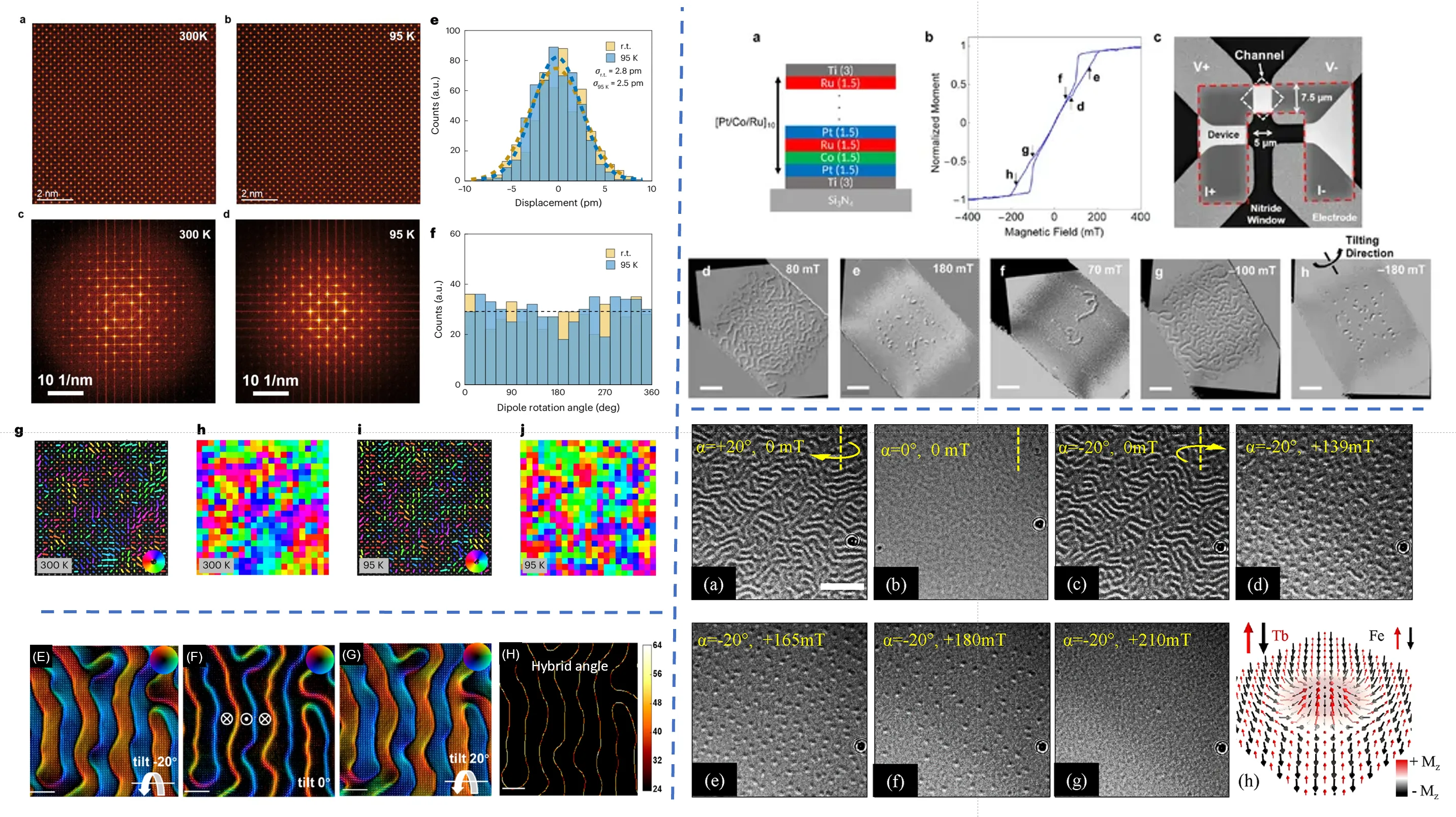
We develop in situ and operando electron microscopy to directly visualize and manipulate materials under electrical, thermal, mechanical, and other external stimuli. Our research focuses on dynamic processes such as polarization switching, domain-wall motion, defect–domain interactions, phase transformations, and interface evolution in functional materials and nanoscale structures. By combining atomic-resolution imaging, electrical biasing, and depth-resolved ptychography, we aim to move beyond static characterization toward real-time observation and controlled manipulation of materials at the atomic scale. Ultimately, we seek to reveal how local structural dynamics govern material functionality and to establish new pathways for controlling emerging states in future electronic and quantum devices.
References
All publications →- Yangyang Si, Denan Li, Yijie Li, … Changsheng Chen, Huaicheng Yuan, et al. Nature Nanotechnology (2026).
- Yuxuan Zhang#, Teng Xu#, Wanjun Jiang, … Zhen Chen*, et al. Nano Letters 24, 2727 (2024).
- Albert M. Park, Zhen Chen, Xiyue S. Zhang, et al. Journal of Applied Physics 128, 233902 (2020).
- Teng Xu#, Yuxuan Zhang#, Zidong Wang, … Zhen Chen*, et al. ACS Nano 17, 7920 (2023).